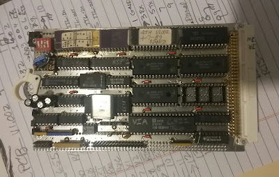
Posts

Showing posts from June, 2018

2 MB DAT PCB

Image
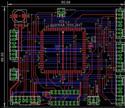
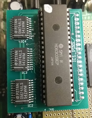
Here is the beginnings of a 2 to 8 MB DAT PCB. Think NoCan series. Update: June/18/2018 I can now edit the schematics and program Lattice 2064A-100LJ84 CPLD's. Here is a beginning of a new "set" of 2MB CoCo3 DAT pcb's. IC on the bottom is the 16x2bit SRAM for $FFAX D6 and D7. Yup, it's a mystery. Actually, these two chips can be added to the "Isolator" pcb making a lot of wiring easier. Older stuff below: Started with a CPU isolator, added 3.3V regulator, and a Lattice lcMACH-4128V CPLD. Not done yet. The blue area under the CPLD is it's own ground plane. I may just make a separate CPLD PCB then wire it to the current Isolator. This PCB creates ZA9 and ZA10 for expanded memory. ZA9 is like the 2MB setup that has been used in the past. The ZA10 portion is new and will expand the memory more than the 2MB. The CPLD has the 16x2 sram inside. Connectors: Upper left is the ZA9, ZA10 connection to the Memory

A MC68008 FIG-FORTH board, off topic.

Image
Yes, a MC68008 FIG-FORTH board, hand-wire-wrapped. You can see the date on the EPROM (4-7-1989). Designed it, wire-wrapped it, wrote the FORTH , tested it. It still works as tested this year 2018. Connects as a RS232 device. Several RAM chips (4), EPROM with FIG-FORTH inside, Ceramic MC68008, SY6551, S6522-VIA, Floppy interface with missing WD1772 IC, RS232 chips. Several PALs that still hold their code. Triple row header for bus connecting. I did find that WD floppy controller chip and it's back in place. The single color wire-wrap side with chip labels. IdeZilla Comments Welcomed

CPU Isolator, 6809E

Image
My first ever $2 JLCpcb came in one day early. After stuffing same, it tests OK with no errors. All pins are buffered, address and controls. The data pins are buffered on the main PCB. After soldering those pins, the extra is removed. Then this PCB is pressed into the socket for the CPU on the main PCB and the CPU is installed on this PCB. IdeZilla Comments Welcomed

512K Ram; with hooks for 2 to 4MB.

Image
The testbed for more RAM started with this hand-wired kludge. It is a half-stick of 16mb x 32 bit PC memory. Yes, it was cut into two pieces and re-wired to work here. Backside of that PCB.  Some Tektronix folks may recognize this board. This shows the half-stick (72-pinner) upside down and wired in. Here it is mounted into a Tandy CoCo3 and being tested. NitrOS-9 (6309E) reported the 512K as useable. This is the hand-drawn schematic to wire that half-stick of memory to the interface board. My second $2 JLCpcb order came in on 5-29-2018 one day early. It looks like this: Mounted into a Tandy CoCo3 it reports 512K. It worked the first time. Only two pin labels were swapped. The 4 chips are 4mb x 4 bits. Address legs A9 and A10 are grounded for now and will be available when the DAT PCB is finished. The drams are hand-soldered